Research
Nanowire Devices - Frolov Lab
Fall 2021 - Fall 2022
For two semesters, I worked as an undergraduate research student under Dr. Sergey Frolov. His lab's primary goal is to realize Majorana Fermions by developing superconducting devices built around nanowires. During my time here, I had the opportunity to gain hands-on experience in nanofabrication techniques, especially those pertaining to condensed matter research.
Some key instruments I received training on were the Scanning Electron Microscope, Plasma Etcher, e-Beam Evaporator, Maskless Aligner, Atomic Force Microscope, Wire Bonder, and Micropositioner
In the summer of 2022, Dr. Frolov Also gave me the opportunity to represent his lab at a partnered lab in Grenoble, France, as part of the GIIP program sponsored GIANT.
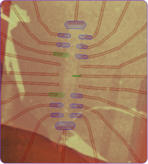
Graphene Heterostructures - NEEL Institute at CNRS
May 2022 - July 2022
For 10 weeks during the summer of 2022, I went to work under Dr. Benjamin Sacepe at the NEEL Institute at CNRS in Grenoble, France. Similarly to Dr. Frolov, Dr. Sacepe's lab also aims to realize Majorana fermions and parafermions with the intent to make progress towards topological quantum computation. To that end, his lab studies superconducting behavior in the edge channels of graphene-based Van-der Waals heterostructures operating in the quantum hall regime.
During my time here, I was tasked with developing a tunneling probe on one of these graphene heterostructures, to empower the lab to more easily measure the density of states in the edge channels. With that goal in mind, I progressed through the following steps of the fabrication process:
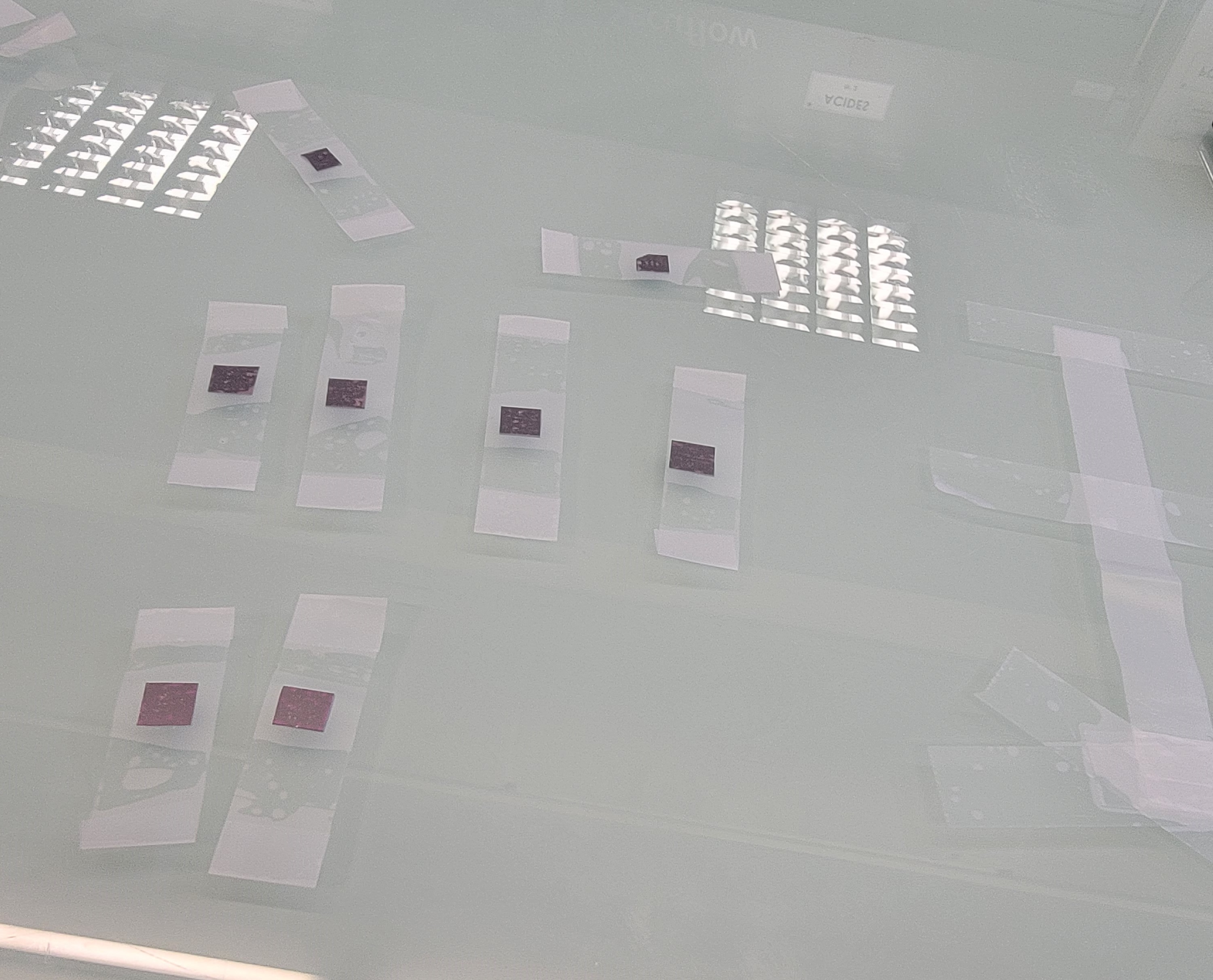
1. I performed exfoliation on graphite and hexagonal Boron Nitride (hBN) flakes
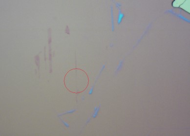
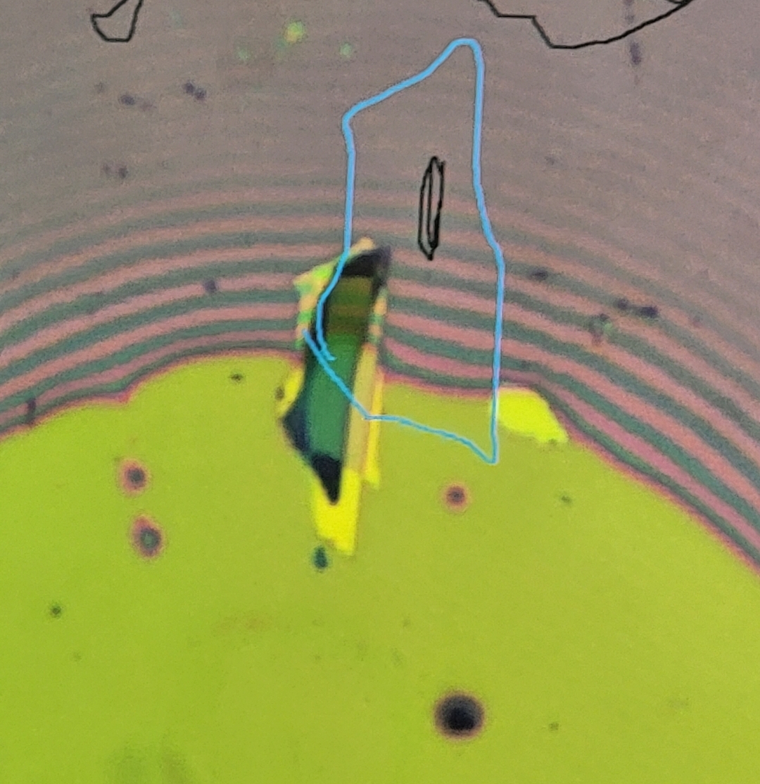
2. Then I would perform optical microscopy on the chips to search for good flakes
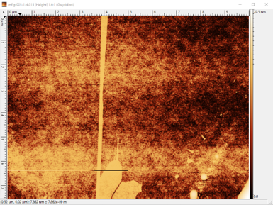
3. Third, I would perform atomic force microscopy on the flakes that look promising
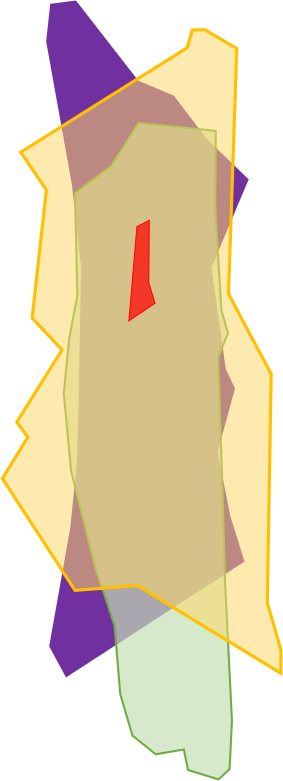
4. I would then organize good, clean flakes into a stack plan, which consisted of top layer hBN, graphene, bottom layer hBN, and finally graphite as a back
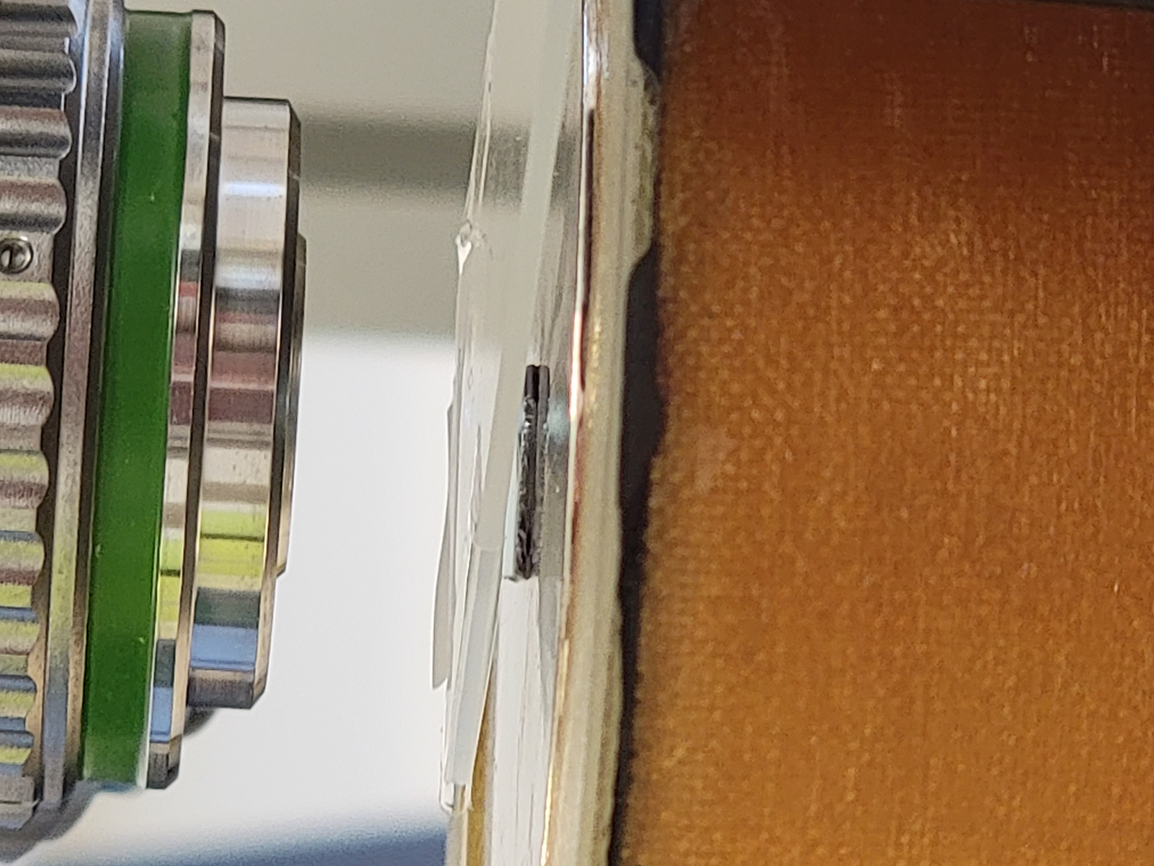
5. Then, I would use a stacking machine to carry out that plan. This consisted of making a thin polymer film, stretching it across a curved stim on a glass slide, and then repeatedly bringing the film in contact with the desired flakes, heating the system to make the film expand and pick up the flakes, and then letting it cool
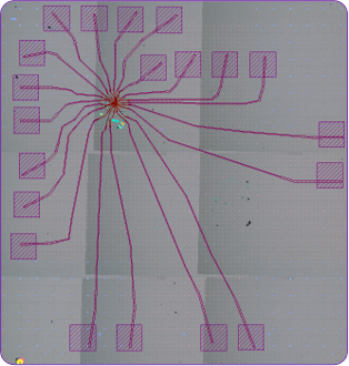
6. If the stack looks viable, then I would design a deposition pattern in KLayout
7. Then I, assisted by colleagues, would iteratively perform spin coating, lithography, deposition, and liftoff to deposite the desired pattern onto the stack
8. After all nanofabrication is finished, the device would undergo electrical testing